
An increasing number of power electronics products are taking advantage of a growing trend in the printed circuit board industry.
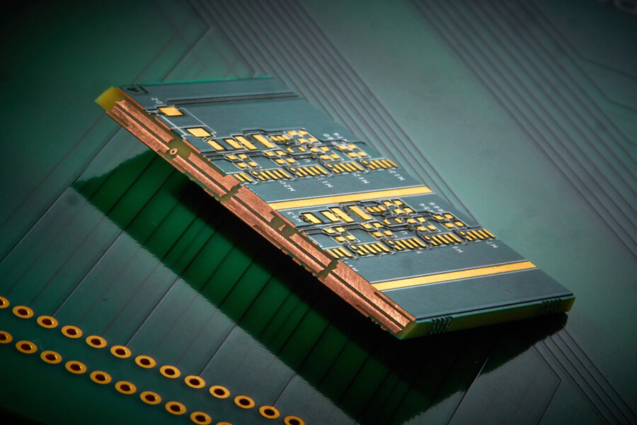
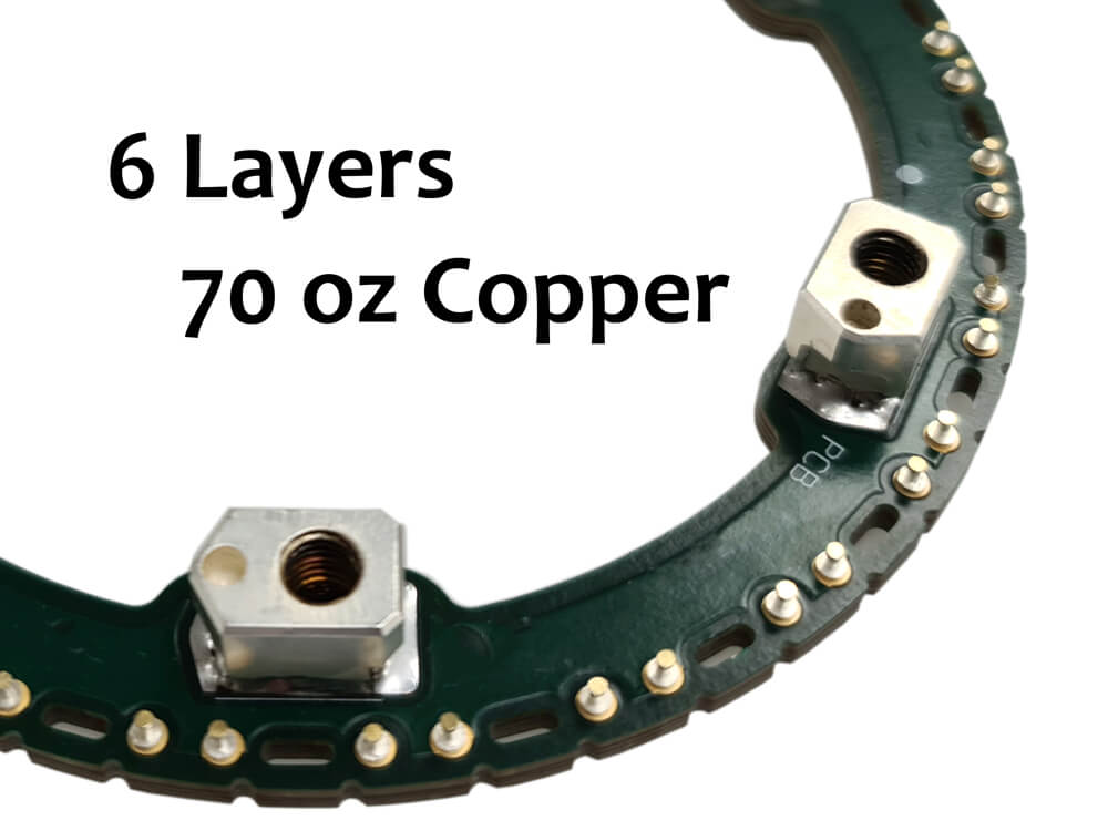
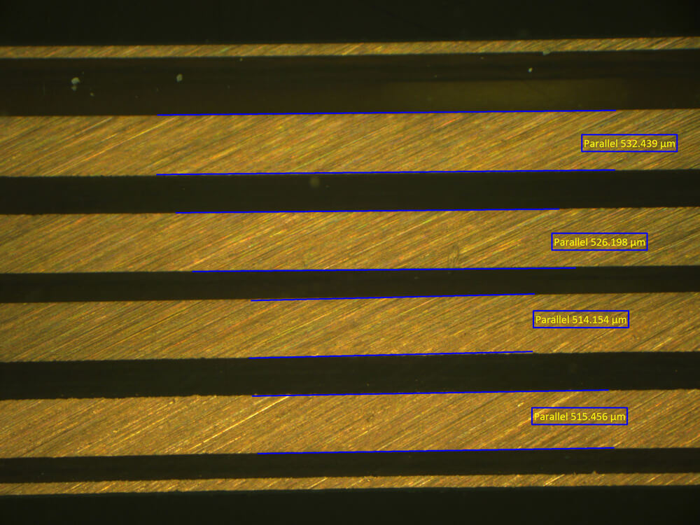
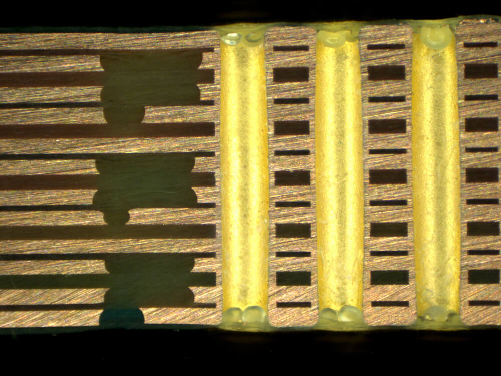
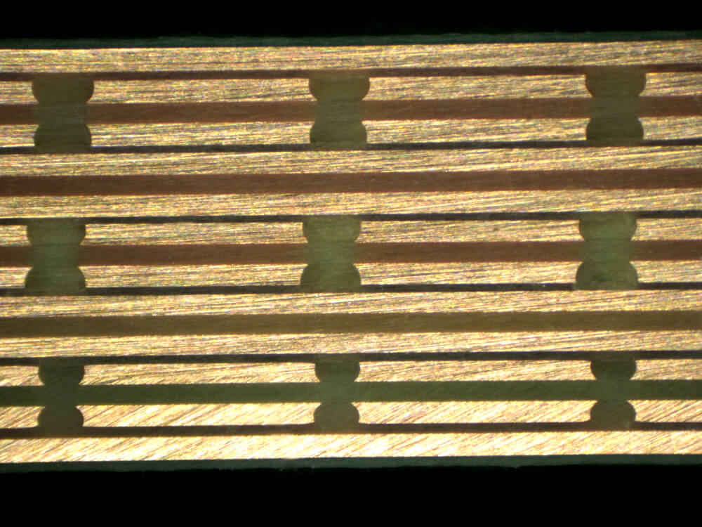
PCBs with 3oz or more of finished copper in the inner and/or outer layers are defined as Heavy Copper. Our manufacturing facilities allow Heavy Copper boards to be produced up to 32 layers.
We also have the capability for Extreme Heavy Copper - up to 30oz per layer for 2 layer applications.
Heavy Copper and Extreme Heavy Copper PCB's offer benefits such as:
Daleba can help you with design procedures for Heavy Copper. We can offer track and gap spacing guidance, current-carrying details and best practice guidelines for heavy copper circuits.
| Property | Weight (oz) | Thickness (mm) |
|---|---|---|
| Standard Copper | ½ - 4 | 0.018 - 0.14 |
| Heavy Copper | 5 - 15 | 0.175 - 0.525 |
| Extreme Heavy Copper | 15 - 70 | 0.525 - 2.45 |
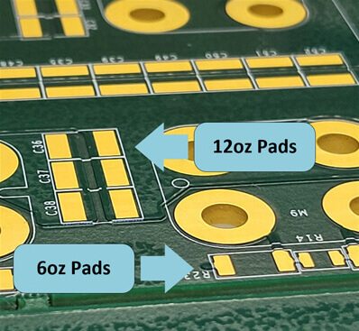
| Mixed Copper Weights | 1 ½ oz and 30 oz on the same layer (Double Sided) | 1 ½ oz and 30 oz on the same layer (Double Sided) |
Applications:
Sign up to receive a monthly PCB newsletter containing the latest information in the world of PCBS including new technology and supply chain information.
Sign up Now
Daleba can manufacture PCBs ranging from single-sided to complex boards in excess of 40x layers. Our in-house CAM engineering resource allows us to rapidly check, panelise and commercially optimise a fast turnaround prototype as well as small volumes. We can supply simple technology boards in as little as 24 hours!


