Ceramic PCB Process Methods & Capabilities

Ceramic production methods and manufacturing capabilities

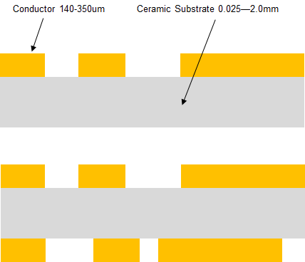
Ceramic PCB - DBC (Direct Bonded Copper)

Ceramic Manufacturing Capabilities document

  • Direct Bonded Copper (DBC) is used when a high copper thickness is required - 140um (4oz)-350um (10oz). Heavy Copper.
  • The copper is bonded to the Ceramic substrate on one or both sides using a high-temperature oxidation process.
  • The copper and substrate are heated in an atmosphere of nitrogen containing about 30 ppm of oxygen; under these conditions, a copper-oxygen eutectic forms which bonds successfully both to copper and the oxides used as substrates.
  • The copper layers can then be etched using standard PCB technology to form an electrical circuit.
  • Laser drilling is then used for any through hole requirements and profile machining.

Disadvantages:

  • Due to the Oxidisation bonding process there can be a slight reduction in Thermal Conductivity created by a void between the Copper and Ceramic layers.
Closeup of Ceramic Direct Bond Copper

Applications:

Main applications are high power modules, like IGBT, CPV, or any other wide bandgap device modules.

  • IGBT
  • High-Frequency Switching Power Supply
  • Automotive
  • Aerospace
  • Solar Cell Component
  • Power Supply for Telecommunication
  • Laser Systems
Closeup of Ceramic Direct Bonded Copper

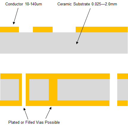
Ceramic PCB - DPC (Direct Plated Copper)

  • Direct Plated Copper (DPC) is the newest development in the field of Ceramic Substrate PCBs.
  • It involves plating the copper conductor layer to the copper substrate under high temperature and pressure conditions.
  • The addition of a thin titanium layer acts as a bonding interface between the copper and Ceramic layers.
  • A very thin layer of Copper is deposited at this stage coating the Ceramic substrate and any pre-drilled holes.
  • Track printing and etching is then performed with the thin Copper allowing for very fine tracks and reduced undercutting.
  • The panels are then plated up to the required end copper thickness.
  • Using this method can result in copper thickness' ranging from 10um (≈ 1/3oz) to 140um (4oz).
  • It also allows for the possibility of plated or filled vias. Something not possible with Thick Film or DBC technology.
  • Different copper thicknesses possible on a single layer - ideal to have a control and power section on one layer.
Ceramic Direct Plated Copper - layers of conductor onto a ceramic substrate

Applications:

  • HBLED
  • Substrates for solar concentrator cells
  • Power semiconductor packaging including automotive motor control
  • Hybrid and electric automobile power management electronics
  • Packages for RF
  • Microwave devices
Closeup of Ceramic Direct Plated Copper

Ceramic PCB - DPC vs DBC

Both DBC and DPC have the same advantages for high power applications, due to the use of a direct bond between Copper and the Ceramic substrate, therefore, the same key attributes for both of them are:

  • Outstanding Thermal Conductivity
  • High operating temperatures
  • Good mechanical strength; mechanically stable shape, good adhesion.
  • Excellent electrical insulation
  • Superb thermal cycling stability
  • Good heat spreading

The differences come when looking at the design considerations and applications. DBC being suited to high current capacity, however limited on circuit design. DPC allowing for finer tracks and through hole connection.

Ceramic PCB - AMB (Active Metal Brazing)

  • Ceramics - AMB (Active Metal Brazing) is a new innovative way of producing Ceramic Substrates without metallisation.
  • In a high temperature vacuum AMB enables copper to be joined direct to the ceramic base.
  • A high reliability substrate with unique heat dissipation properties.
  • Brazing technology enables copper weights of up to 800µm on thin ceramic substrates.
  • Ideal for Power Electronics applications

AMB Single Sided

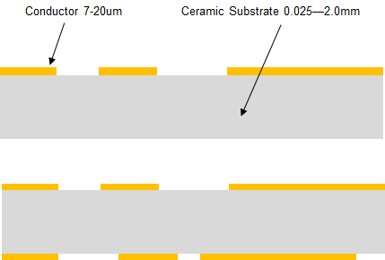
Various copper weights are available to meet match substrate thicknesses detailed in the table below. It is recommended the copper thickness on any design is no more than half the ceramic thickness.

AMB double sided

Double sided substrates offer greater mechanical strength and stability enabling Heavy Copper to be offered on thin ceramic substrates. The following is a guide on double sided material availability although during the etching process original copper weights can be reduced.

Active Metal Brazing Double Sided Panels
  200µm 250µm 300µm 400µm 500µm 800µm
0.25mm SiN
AlN
SiN
AlN
SiN SiN SiN SiN
0.32mm SiN SiN SiN SiN SiN SiN
0.38mm AlN AlN AlN      
0.63mm AlN AlN AlN AlN AlN  
1.00mm AlN AlN AlN AlN AlN AlN
Copper Thickness
Ceramic Thickness

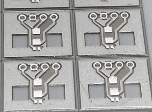
Ceramic PCB - Capabilities

Property DPC DBC
Compatible Substrates Al2O3 / AlN / SiN Al2O3 / AlN / SiN
Substrate Thickness (mm) 0.25/0.38/0.5/0.635.1.0/1.5/2.0 0.25/0.38/0.5/0.635.1.0/1.5/2.0
Copper Weight (µm) 10 - 140 140 - 350
Panel Sizes (mm x mm) Standard: 115 x 115mm
Special: Up to 170 x 250mm
Standard: 115 x 115mm
Special: Up to 170 x 250mm
Finish Options ENIG/ENEPIG/EPIG/Immersion Silver/Immersion Tin/OSP ENIG/ENEPIG/EPIG/Immersion Silver/Immersion Tin/OSP
Min Track Width (mm) 0.1 Dependant on Cu Weight
Minimum Hole Dia (mm) 0.08 0.08
Plated Via Aspect Ratio 5:1 N/A

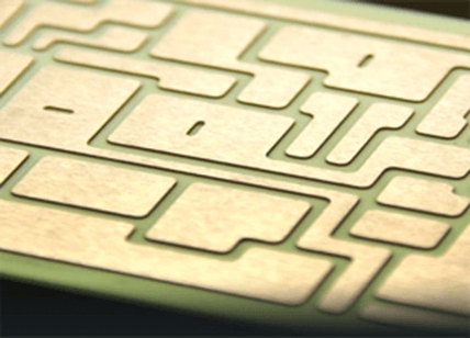
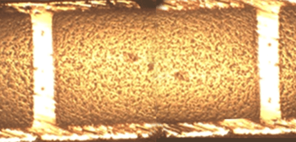
Ceramic PCB - Thick Film

  • Thick Film technology involves the addition of layers of conductor (Copper or Silver) onto a Ceramic substrate via screen printing processes.
  • Suitable for use with Al2O3/AlN and Sapphire substrates.
  • A cost-effective solution with fewer manufacturing processes than other methods.
  • With a conductor thickness between 7-20um it is not well suited to power electronics requiring high current capacity.
  • Due to conductor application it is also unsuitable for designs requiring fine tracks and/or plated/filled vias.
Closeup of Ceramic Thick Film
Ceramic Thick Film Technology - layers of conductor onto a ceramic substrate
Joscar Registered